

I purchased a KN-Q7A kit from crkits.com in China. The kit is well made and the instructions are excellent. It is a low cost and light weight SSB transceiver for 40m. Naturally to keep it simple and keep the cost down, there are trade-offs in the design. There are three elements that were a concern for me:
- The VXO frequency control has very limited coverage (about 20kHz) and is susceptible to significant drift as the radio heats up. This makes it hard to know exactly what frequency you are on and is noticeable enough that the beginning to end of a SOTA activation resulted in comments on the drift from chasers.
- The final PA has relatively high IMD products which I measured at around -10dB to the signal peak on a two-tone test. This seems to be caused by a number of issues. While it is readable, I prefer to have a cleaner signal.
- The minimum operating voltage for the rig can be over 11V due to the 7808 regulator and reverse battery protection diode combination.
I wanted to keep the compact case and the excellent receive current drain (about 60mA) as far as possible, so resolved to squeeze everything into the upper portion of the existing case.
New regulator
The problem with the 7808 regulator is that its dropout voltage is up to 2V. When combined with the nearly 1V drop on the reverse battery protection diode under transmit current levels, then the 8V rail regulation stops when the battery gets to around 11V. This is too high for driving with 3S LiPos which can be drained to around 10V.
This is relatively easy to solve with the replacement of the 7808 by an LDO regulator. In my case I chose a LM2940-8.0. It requires a 22uF tantalum capacitor directly across the output for stability and a SMD capacitor fitted nicely.
I also changed the reverse voltage diode to a power schottky diode. The transmitter now works down to an input voltage of about 8.5V which is excellent.
VXO replacement
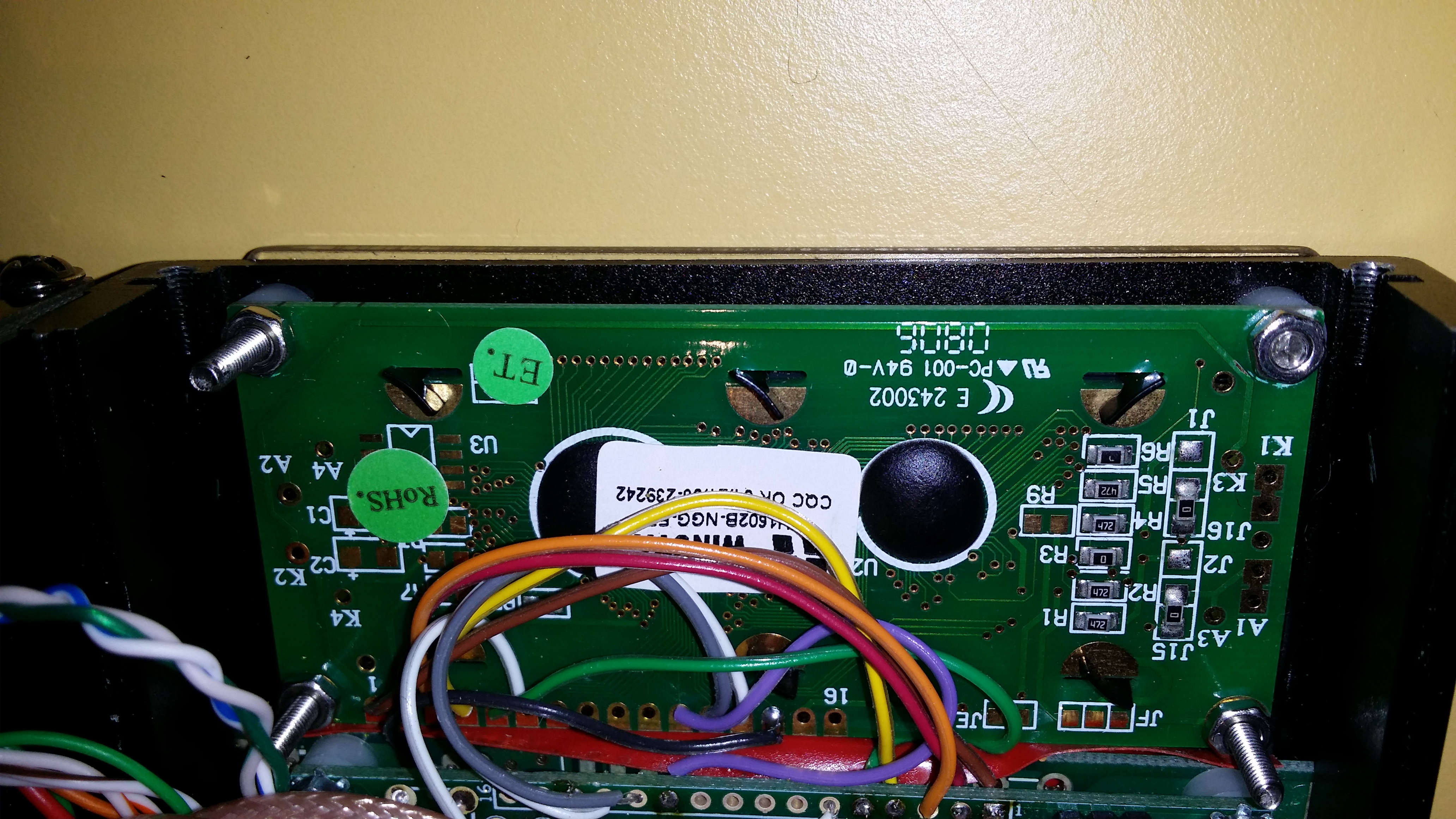
The obvious solution to a better VFO was to go with a modern DDS. As it happens there is an excellent kit available from N3ZI. I built this and added a non-backlit LCD to keep the current draw as low as possible. The output of this module can be fed directly to the oscillator input of the LO mixer. This provides full coverage of the 40m band.
The BPFs in the rig are optimized to be only about 150 kHz wide, so a little narrow to cover the whole band. I modified these by replacing the 2pF middle capacitor with a 3.3pF capacitor. This widened the coverage somewhat, but beyond 7.150MHz, the response drops down a few dB.
I was concerned that the digital electronics might interfere with the RX, but so far have had no noticeable effect other than a mild clicking as the rotary encoder is turned.
The RX current drain has increased to just 120mA (about 1.5W) which would run for 18 hours on a 2200mAh LiPo! Here’s a couple of photos of the completed modification.
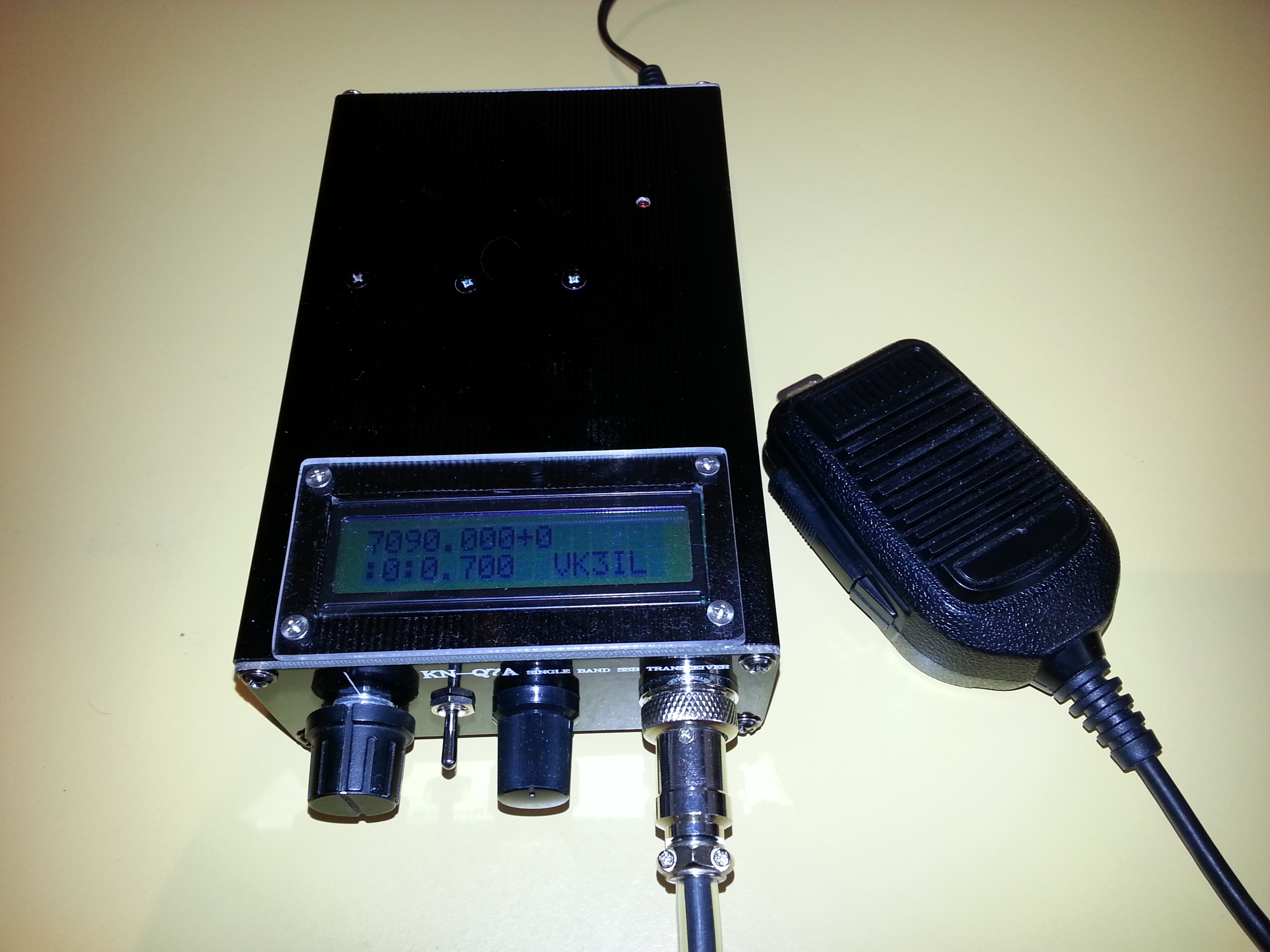
Modified KN-Q7A showing the new frequency display.
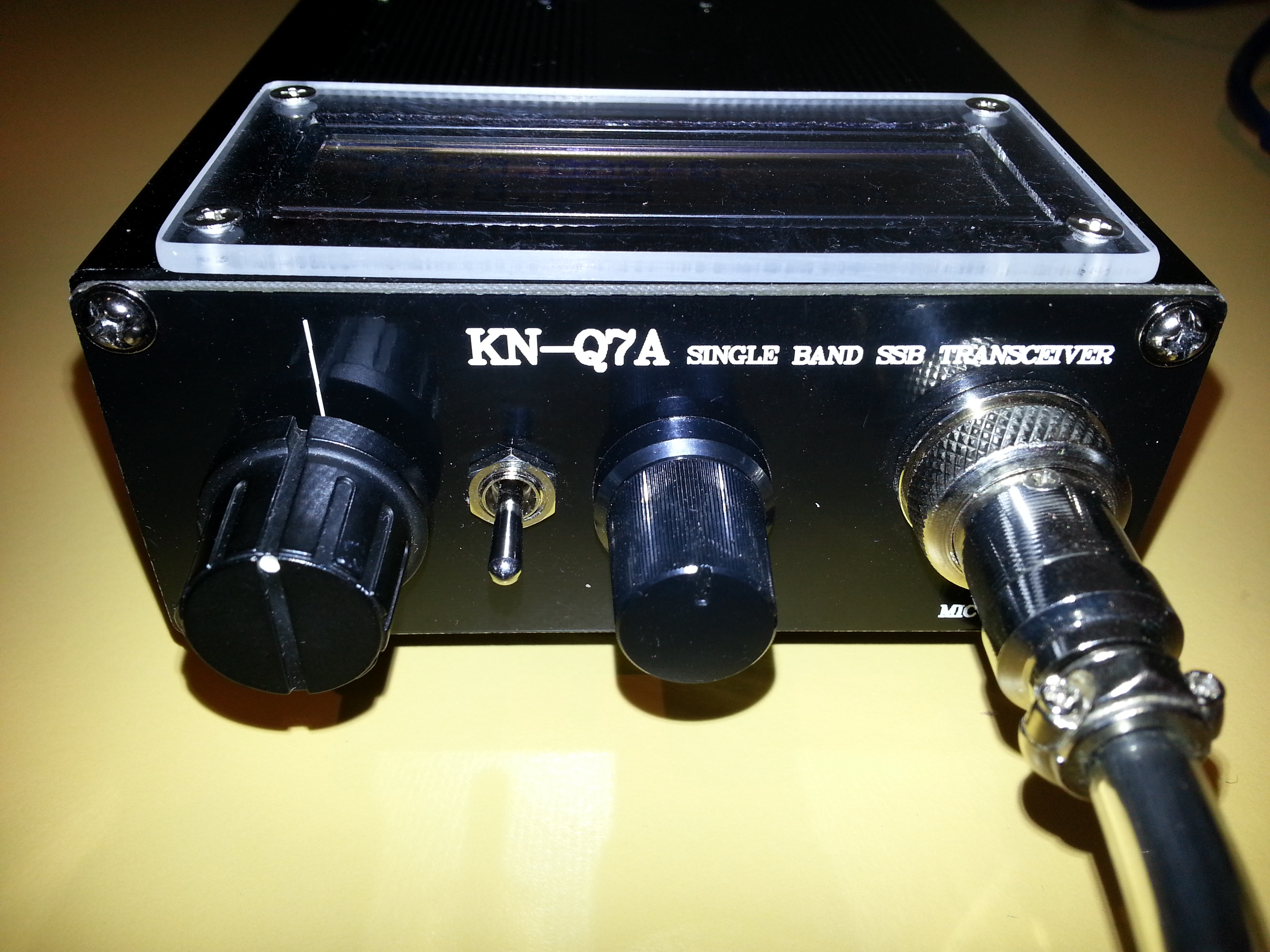
Front panel of modified KN-Q7A. The tune knob on the left is now the rotary encoder for the DDS. The additional toggle switch is the memory selector for the DDS.
New PA stage
When I explored the IMD performance of the rig, I found it fairly mediocre. 3rd order products were about -10dB to the tones which is not great. Some of the IMD seemed to be coming from the final PA stage with smaller amounts spread across the earlier stages.
The rig uses a single IRF640 MOSFET for the final PA which, as a switching transistor, is not really designed for linear applications. I decided to implement a separate new PA stage and then reduce the drive level to the point where a cleaner output resulted.
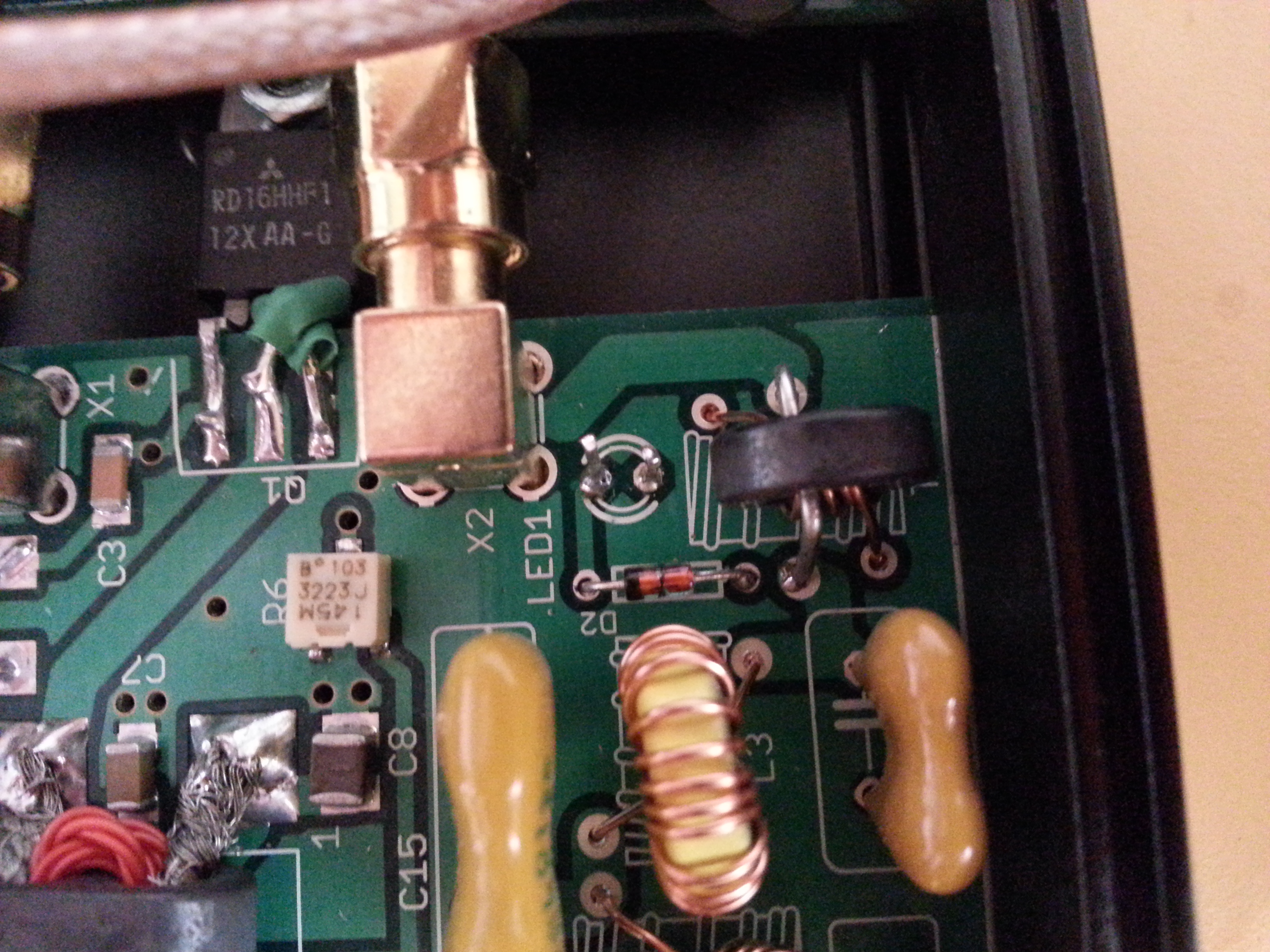
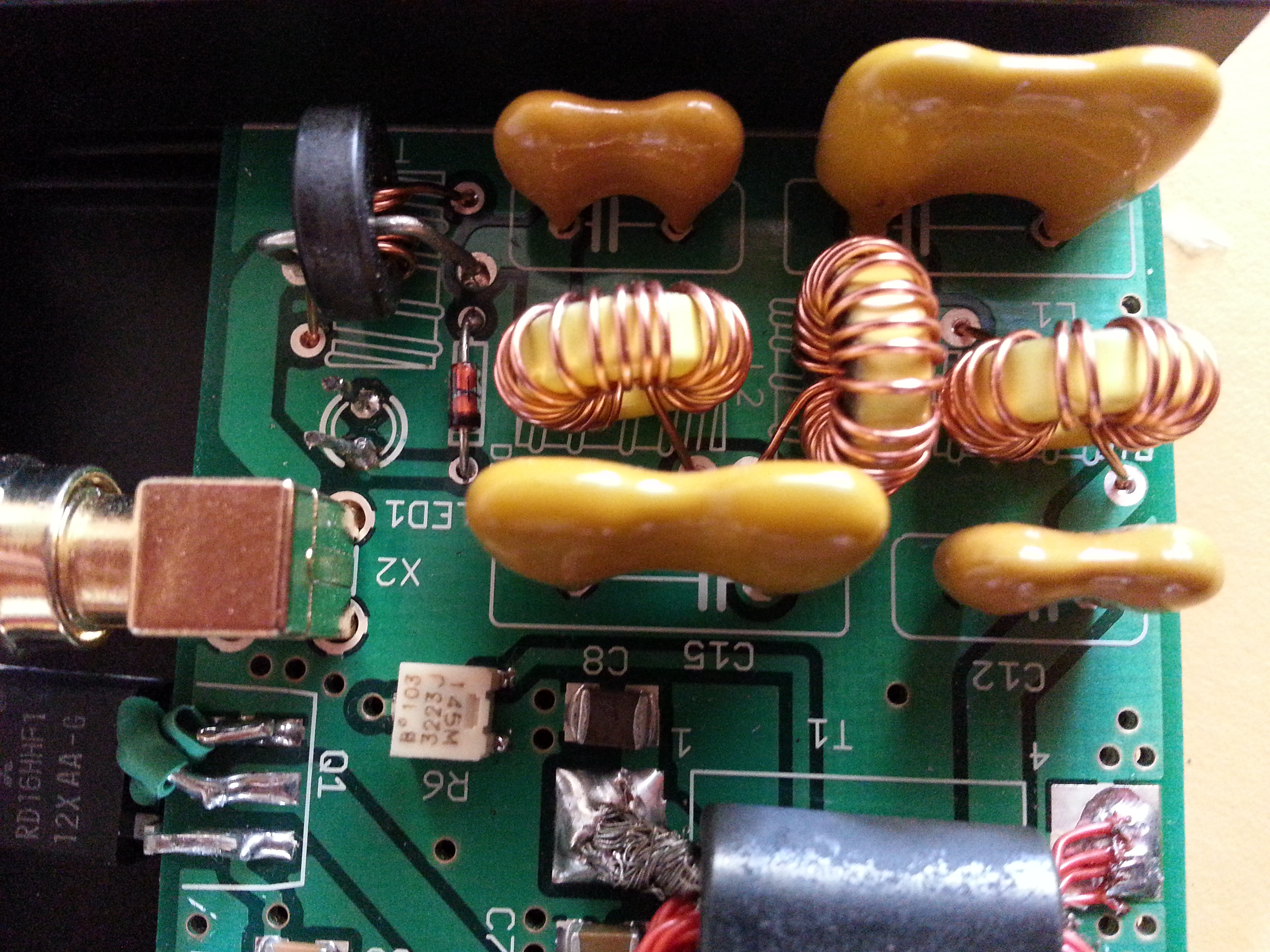
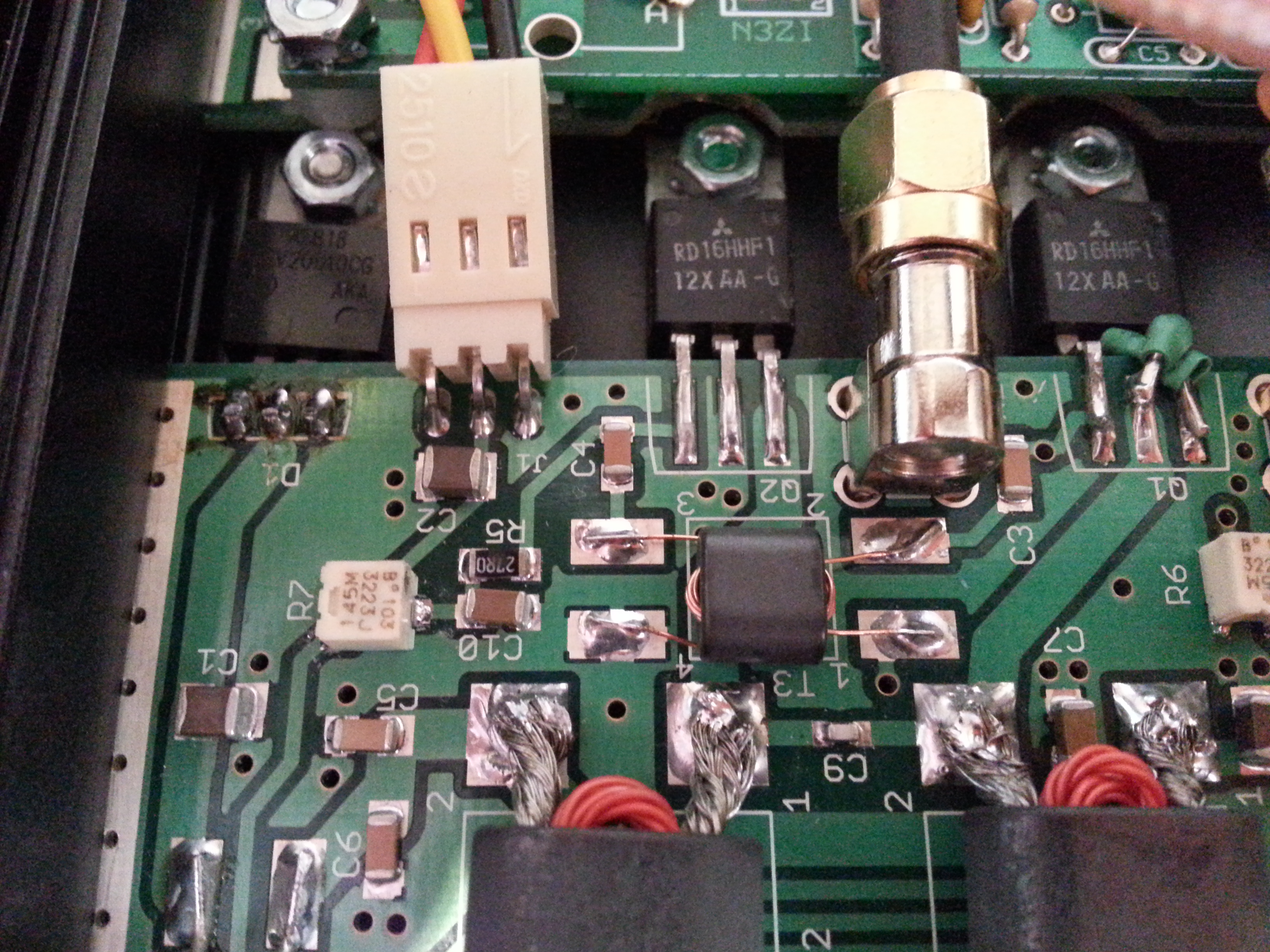
I decided to re-design the final PA to use RF MOSFETs (RD16HHF1) in a push-pull configuration. The design is borrowed almost directly from Loftur Jonasson (TF3LJ/VE2LJX). To his design I added a LPF based on the work of W3NQN. I also added a transmit current monitor to provide a very compact way of monitoring the transmitter output – useful for identifying antenna or other faults in the field.
Here’s the final schematic and PCB layout:
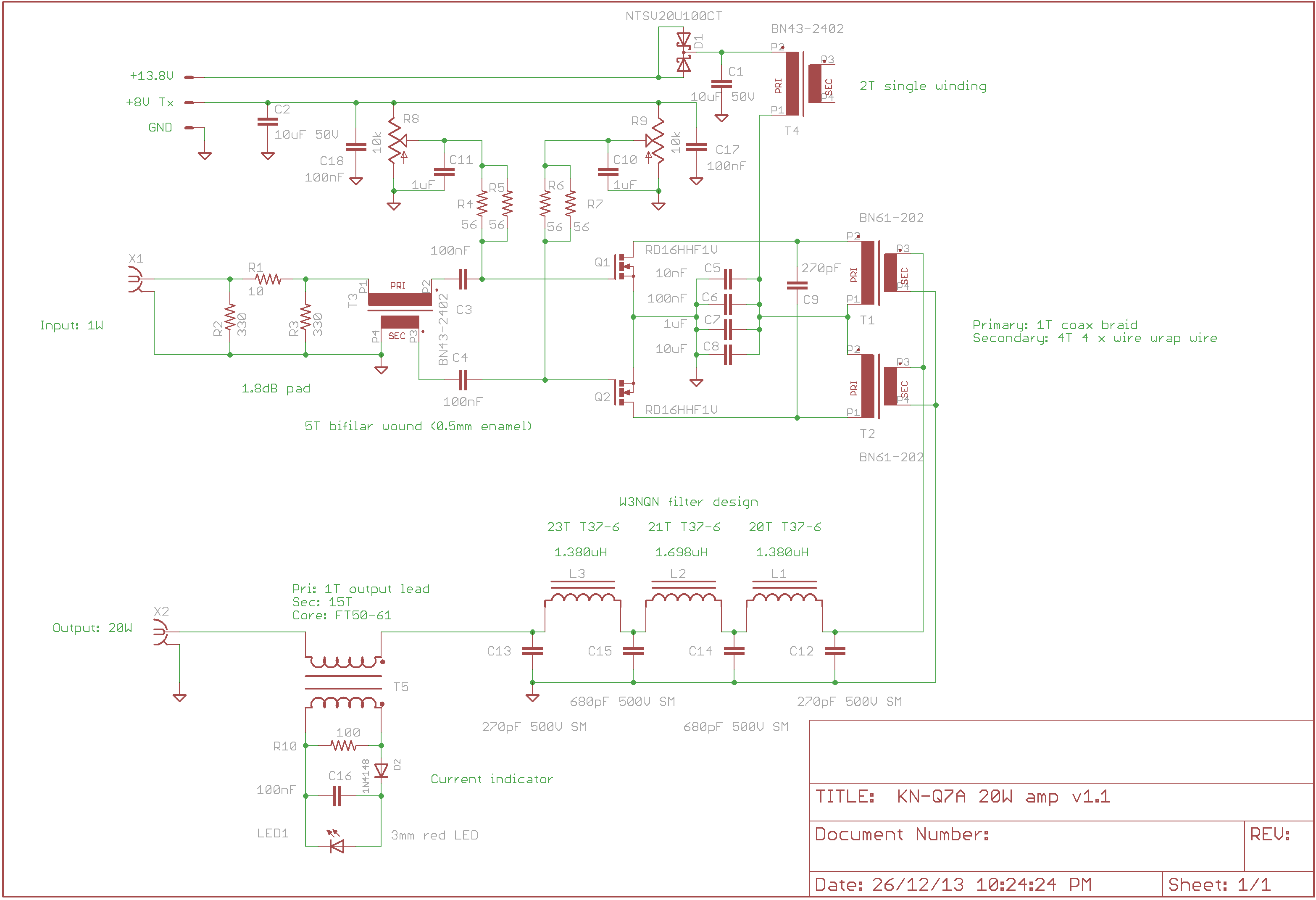
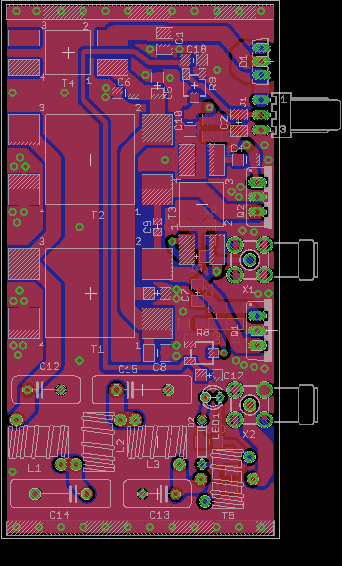
The PCB is designed to fit neatly into the slots in the upper section of the case in much the same way as the main PCB. The MOSFETs and the Schottky diode are bolted to the case for heatsinking. The LED is installed on the back side of the PCB and protrudes through a small hole in the lid of the case. The amplifier is inserted between the output of the existing LPF on the main board and the T/R relay.The +8V bias supply is taken from the +8VT line on the main board to ensure that bias is only applied during TX. Bias is set to 450mA per MOSFET, which is significantly higher than the 60mA for the main PA. However, as it’s only biased during TX, in practice it does not significantly increase the battery drain overall.
The output of the existing rig needs to be dropped substantially to about 1W input to the new amplifier module. This is achieved by reducing the microphone drive level significantly by changing the 10k electret mic bias resistor to 3.3k.
The new amplifier is capable of approx 20W output at 13.8V drawing 3.7A (with a 42mVp-p sine wave at pin 2 of the modulator). The measured overall rig efficiency is 42% which is OK for this class of amplifier.
There is no bias stabilization in the circuit and the bias current does change significantly as the MOSFETs heat up. However, this does not appear to affect linearity or lead to a runaway condition and so is deemed acceptable. A thermistor/resistor to ground could be added to the bias circuits if this became a problem.
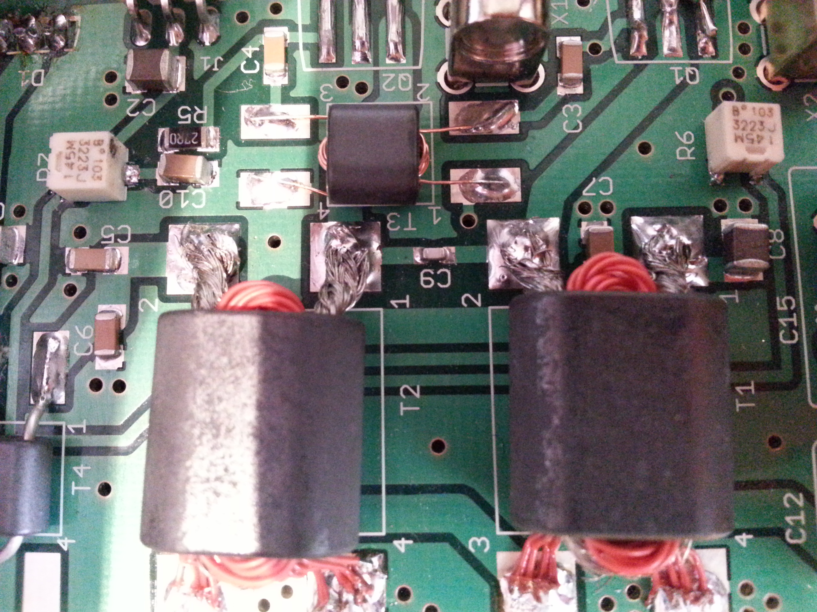
One other source of IMD that was identified was T3, the original output stage impedance matching transformer. This is a 1:4 transmission line transformer stepping up the output of the final PA transistor to 50 ohms for the final LPF. As originally constructed, this was 5T on a FT37-43 toroid. It appeared to be generating several dB of IMD, potentially due to there being insufficient reactance to prevent normal transformer mode operation. It was also getting extremely hot (>100 deg C after 10 min carrier).
Reading about transmission line transformers indicated that in power applications, low permeability cores are preferred and that type 61 material had much lower loss than type 43 and so I re-constructed this transformer as 15 bifilar turns on a FT50A-61 core. This seems to have removed this source of IMD and temperature rise is no longer a problem.
Measured 3rd order IMD is now improved to: -16dB at maximum output – this is still only average, but much improved over the original. The transmitted audio is, while not completely clean, at least quite intelligible and is not splattering.
There output spectrum is very clean with no measurable harmonics to the -60dB level and BFO products are less than -47dBc:
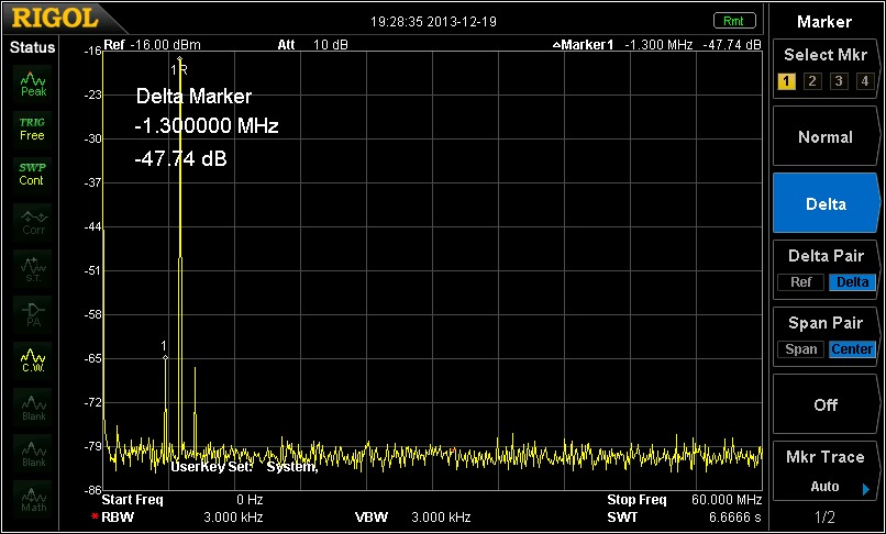
Spectral view with single tone carrier at 20W output and 13.8V supply. Note that all spurious products are better than -47dBc.
The design is fairly conservative and the amplifier will cope with continuous carrier for 10min without overheating. The case gets to about 50 deg C after this time, but this is quite extreme and should pose no problems in normal use for SSB or digital mode QSOs.
Here’s a few photos of the completed amplifier (note that this was the first iteration of the PCB which had a couple of minor errors in it): 
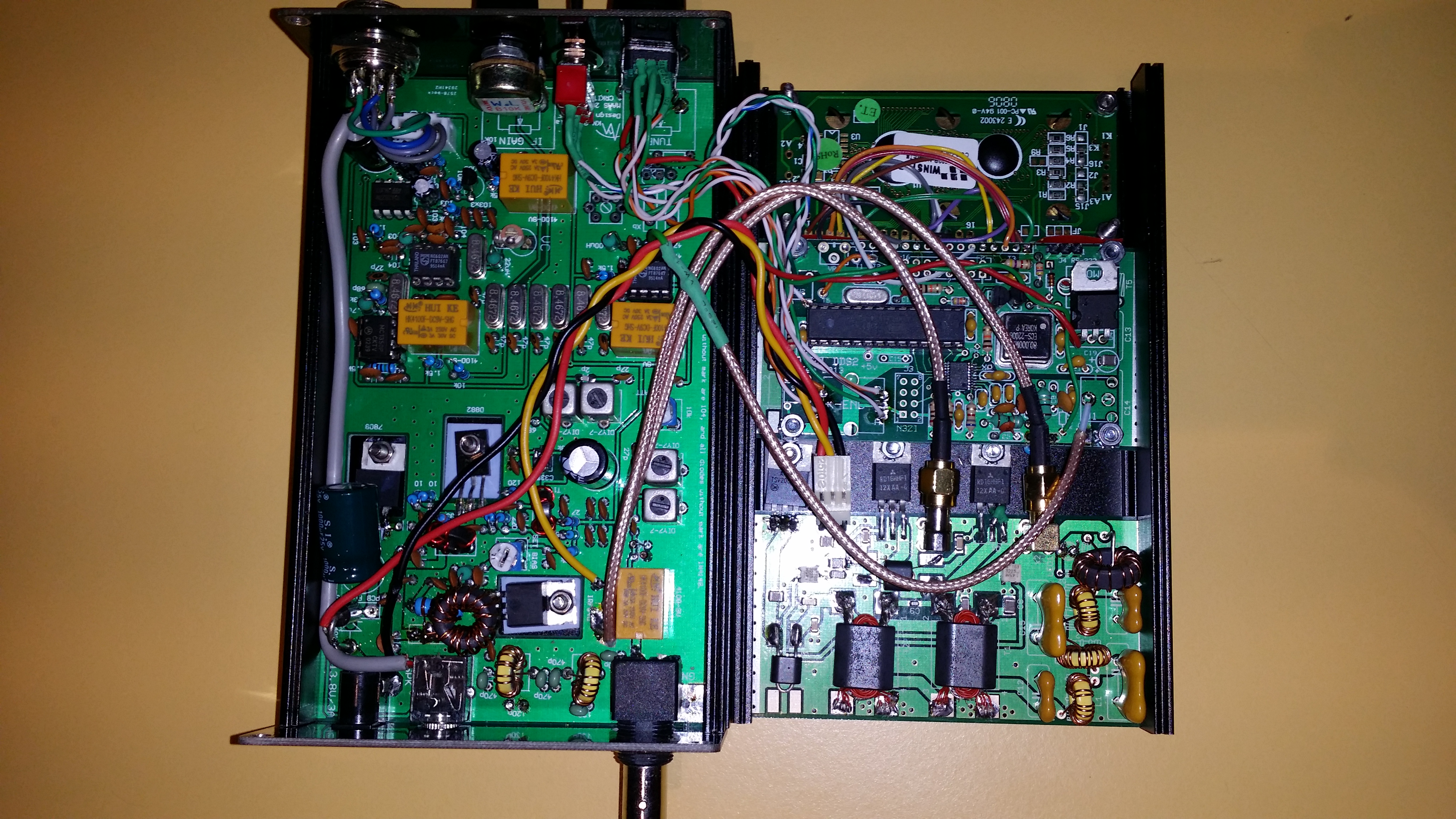
Whole radio – original components on the left and DDS and amp on the right.
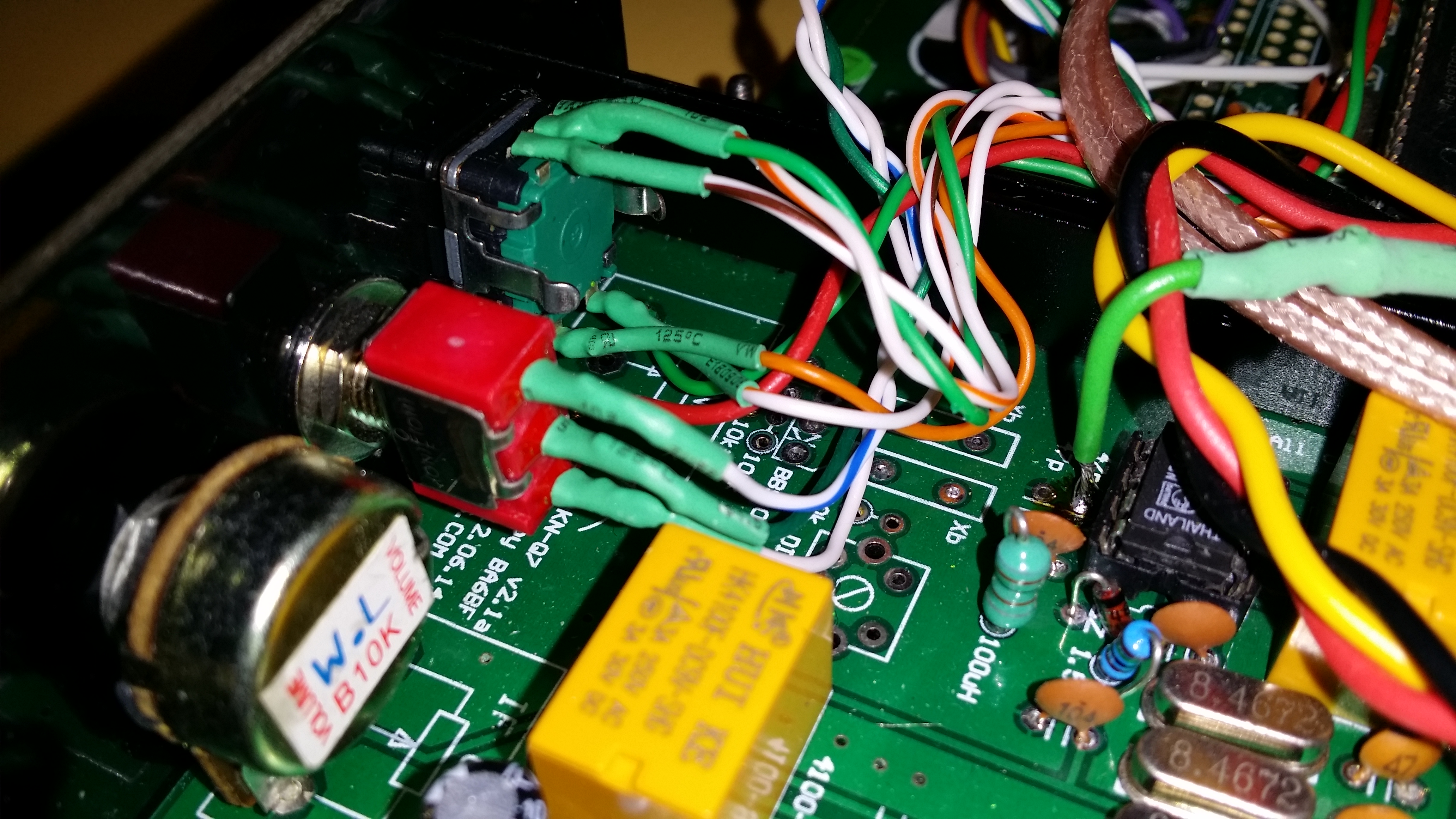
Connection to rotary encoder and switch. Note all components from original VXO have been removed.
The whole lid with DDS display, DDS board and amplifier board

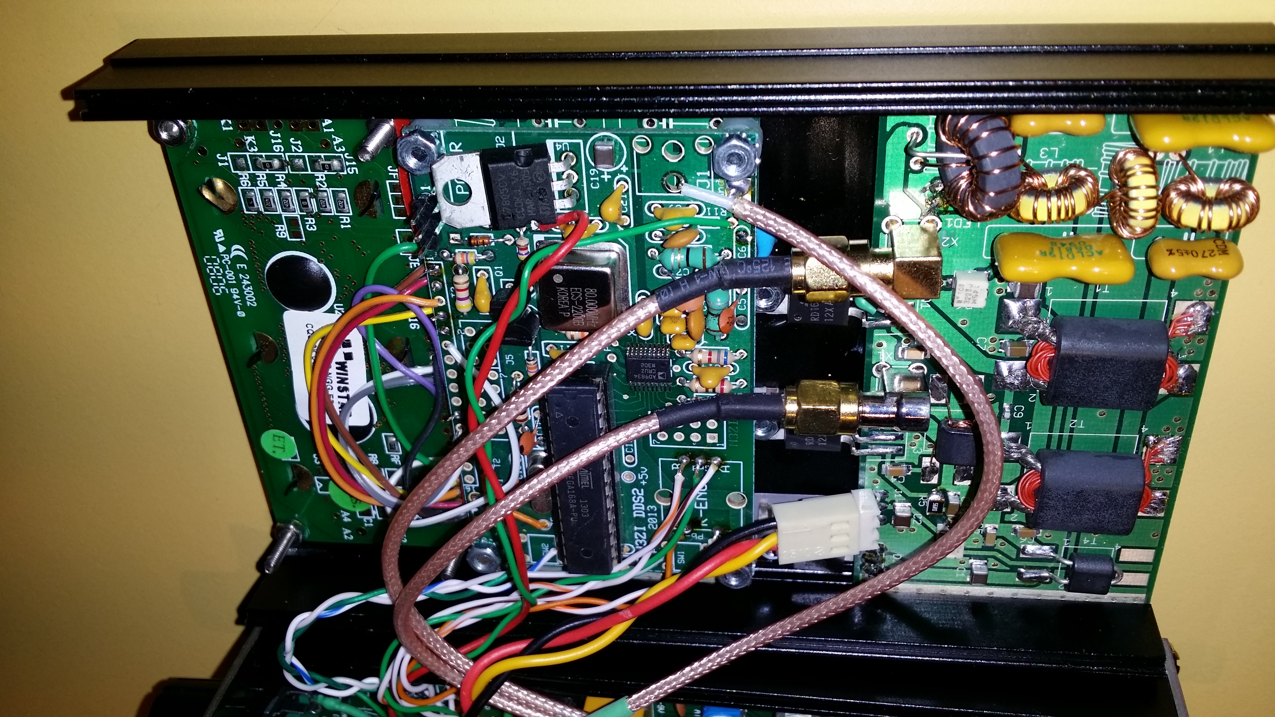
DDS board attached to a plain board secured by slots in case.
Display for DDS
Update June 2014 – Adding AGC to the rig
The biggest practical issue I’ve found in using this transceiver is the lack of AGC. Turning the gain up to hear a weak station only to be blasted by a higher power station gets tiring!
I’ve recently discovered a neat little mod kit for the X1M transceiver to add AGC to it. The mod was designed by Dale W4OP and is described here: X1M AGC mod and here: X1M AGC mod manual. It was available as a kit from W5COV’s “QRP Fun” (site no longer seems to exist).
The mod is basically an audio-derived AGC amplifier the output of which is fed into pin 5 of the MC1350 IF amplifier (its AGC control pin). In the KN-Q7A, the AGC pin of the MC1350 is connected to the IF gain pot as the means to control the IF gain of the rig. The X1M has a fixed IF gain and variable AF gain, so the mod is setup to change the X1M IF gain to be driven from the AGC amplifier and the AF is picked up before the AF gain control (see the manual above).
In the KN-Q7A, there is no AF gain control. I found that using the input to the audio amplifier as the pickup point did not work for this rig as it loaded down the product detector/modulator and seriously reduced the output power on TX. Hence I modified the mod to reduce the gain of the AGC amp to unity and picked up the audio on the output of the AF amplifier – specifically the top of the 10 ohm resistor that forms an output high frequency shunt on the audio output. Reducing the amplifier gain to unity is simply a matter of adding a 50k resistor in series with the AF input (at W3 on the mod schematic).

Here’s the connection to the AF amp output. The easiest point to pick it up from is the top of the 10 ohm resistor that is part of the high frequency shunt filter on the output. Check that the loop at the top of the resistor is not the ground end of the resistor!
To connect it to the KN-Q7A MC1350 chip and retain gain control is simply a matter of removing the 10k resistor between the IF gain pot and pin 5 of the MC1350 and connecting the pot side of the resulting gap in the circuit to the wiper pad on the mod circuit board (you don’t fit the pot supplied in the kit as the IF gain control replaces it). The MC1350 pin 5 side of the gap goes directly to the W4 pad on the mod board.
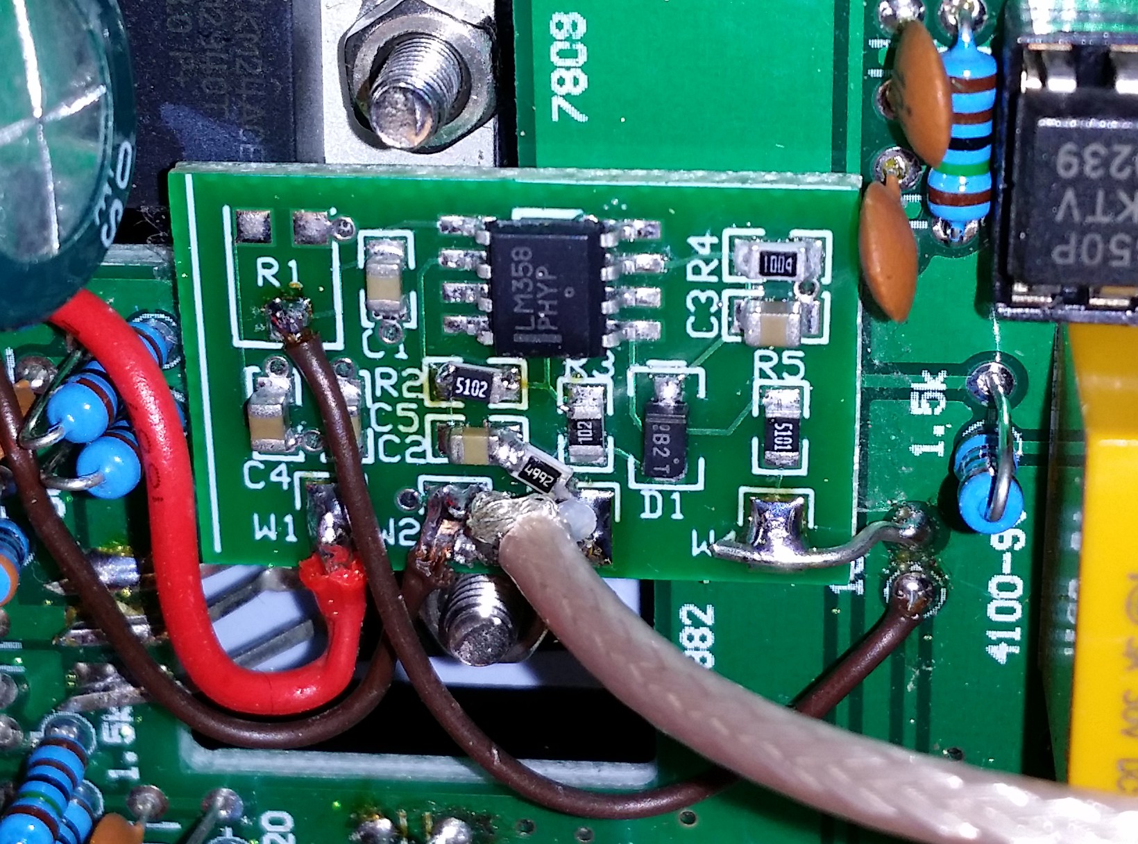
Here’s a close up of the AGC amp board showing the additional resistor added between C2 and the input pad (cut the original trace). You can also clearly see the connection to the pads where the 10k resistor was removed.
The +9V supply pad on the mod connects to a convenient +8V pad on the KN-Q7A and of course Gnd goes to Gnd.
I used shielded wire to connect the lead from the AF amp back to the AGC board to avoid unwanted coupling (shield only connected at the AGC board end).
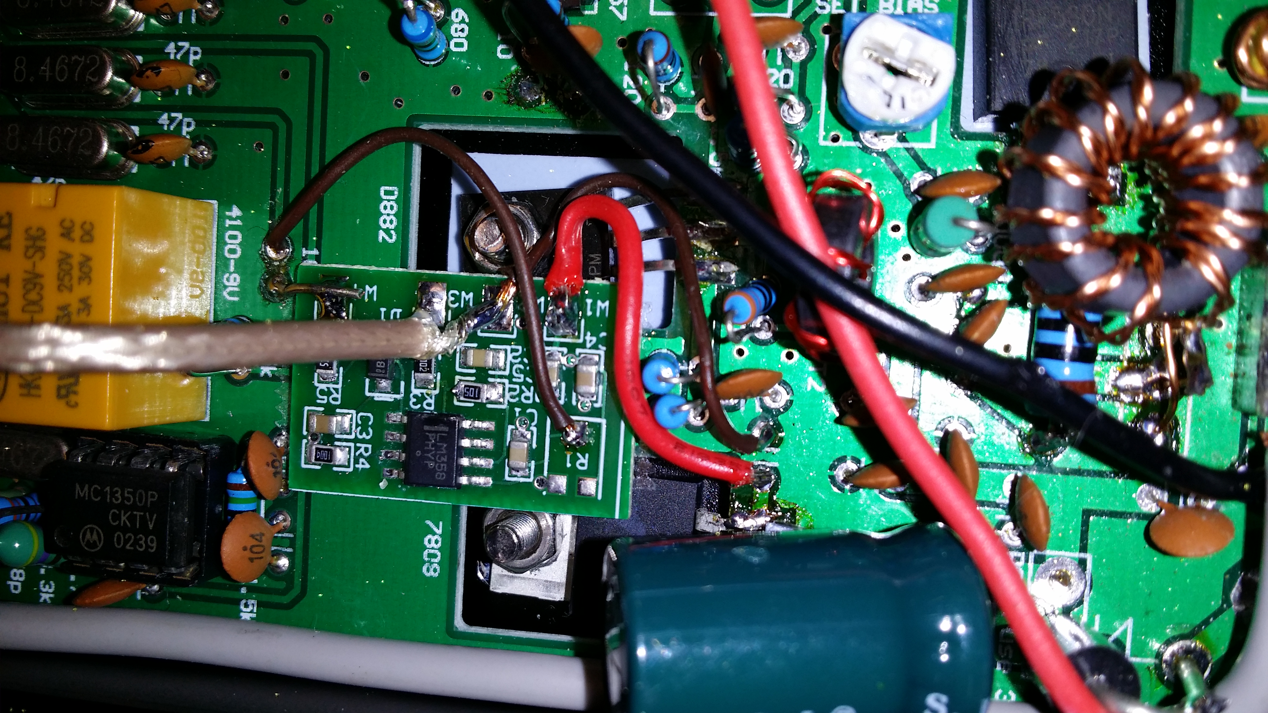
Here’s the AGC board attached to the main board with double sided tape. The power wires connect to convenient pads and you can see the shielded cable going to the audio amplifier pick up point.
Using AGC is simply a matter of setting the IF gain pot to a suitable level (around mid-range) and letting the AGC do it’s job. You can effectively disable the AGC by turning the IF gain to maximum.
Being audio derived, there is a delay in reducing the gain which leads to a brief thump when a high level signal is received before the AGC kicks in. The only cure for this would be to use an RF source for the AGC which is more complex to implement.
The kit board fits very neatly with double sided tape between the voltage regulator and the driver transistor.
This has been a worthwhile improvement to the rig.
I’ll add some comments on how it performs in real usage in due course…
Great job on redesigning aspects of the original rig and turning it into a much better one.
Andrew
vk1da
Pingback: Blue Rag Range and VK3/VE-024 - 5 April 2014 | VK3IL BlogVK3IL Blog
I have one of these on the way and everything I am reading indicates that the 2 weaknesses are No AGC on RX and No ALC on TX.
Wondering if you have considered an ALC Pre-amp between the Mic and the 602 Mixer and if it would be a worthwhile mod – something like what is described in https://electronicdesign.com/analog/effective-agc-amplifier-can-be-built-nominal-cost
And I also plan on using the ILER DDS to give full band coverage.
Hi Bob,
I’d add the other 2 weaknesses I mentioned in the blog – poor IMD and poor frequency stability (which you’ll fix with the DDS)! I didn’t consider an ALC very long because I think this would exacerbate the IMD problems if you were not careful. If it was adjusted to keep the peak-peak output under 200mV, it may provide a useful compression benefit. RF compressors are generally regarded as more effective – see for example:
https://jwm.de/afu/0ft817eng.htm
If you wanted to go the audio route, the following from AD5X may be worth a look as even simpler to implement: https://www.ad5x.com/images/Articles/SSM2165.pdf Not sure if you can get that chip now though.
Since I’ve added the 20W amplifier, I’m quite happy with the output of mine now, so probably won’t add this mod (particularly given I’ve run out of space inside the case!)
I’m still tempted to add audio AGC, as a strong signal can be painfully loud if the gain is turned right up – I definitely wouldn’t risk headphones with this rig.
I’d strongly encourage you to make the change to T3 I outline in the blog to improve the IMD. The wider power supply range mod is also a simple change.
Thanks – was going to look at this as well as swapping out the 2p with a 3.5p cap in the front-end as well. Can you recommend where to get the replacement Core for T3 from?
I have not even got it yet and planning on all the mods 🙂
Also found a neat little Audio AGC at https://rheslip.blogspot.com.au/2012/04/tda7052a-audio-amp-with-agc-and-mute.html that might be simple to implement as a replacement for the current audio output stage.
Bob,
The core for T3 came from RS components. It’s Fair-Rite part no.: 5961001101. Here’s the RS components link: here. You have to buy 10, but they’re not too expensive and shipping is free.
That’s a neat circuit and may be very easy to replace the TDA2822 with. I suspect the circuit would need tweaking to get enough drive for a speaker. I’d try running it off 8V instead of 5V and perhaps using two white LEDs in series to get the output volume up a fair bit. The suggestion of tying pin 4 to 5V through the 10k resistor would probably be needed too to keep the gain up (although I’d add a series diode to keep the max voltage on pin 4 comfortably below the 8V limit). The gain of this amp is 35.5 dB vs 39dB in the current amp – it may make very weak signals hard to hear, definitely worth an experiment though!
I note that RS has a SMT version of this chip which would fit nicely on a small PCB header I think.
Pingback: 40M SSB Transceiver kit | VK5FO
Hi,
Thanks for your nice article about the kn-q7a. I am also an owner of kn-q7a. I have the intention to put inside a dds. Could it be possible that you take some internal pictures with DDS fitted in order to see how you have implemented it?
Best regards
Alex
Hi Alex,
Yes. I’ve updated the entry with a few more photos that hopefully will help. The output of the DDS can be fed straight into pin 6 of the NE602. It’s not too hard a mod, but a bit of re-wiring is needed. Has been working very well for me.
73
David.
Hi David,
Thank you very much for internal view. I will try to reproduce the dds part.
Best 73
Alex
Hi David,
Thanks for reply. I have another question regarding the DDS from N3ZI; I have seen that you have implemented a small switch on the front of your kn-q7a in order to use some feature of the dds. Could it be possible to use only the rotary knob for using the dds like a VFO ? Is this swich neccessary for normal VFO operation ( like step selection ….)
best 73
Alex
Alex,
I think the switch is optional as it’s only used to select the memories on the DDS. The step size selection is done with the push switch integrated into the rotary encoder. The benefit of the memories is to provide an easy way to move up and down the band in large jumps. In practice, if you’re only staying in one area of the band, then the VFO alone is adequate. Check the manual for the DDS though, I may have forgotten an important function.
73
David
Hi David,
I have done on my side the dds mods with the n3zi dds. I have wired all and it seems to works nice. To my surprise I found the modulation on RX not so good. The bandwith seems to be lower. I have try to change the VC in order to have better modulation but It seems not as good as with the VXO. Do you have any suggestion? any help would be welcome
Alex
Alex,
Not sure how changing the LO would affect the receive audio bandwidth (I assume that’s what you mean by “modulation on RX”). I didn’t find any difference when I changed from the VXO to the DDS. Did you perhaps knock the BFO trimmer in the process ? Maybe go through the RX alignment procedure again to be sure. Not sure what you are referring to by the “VC”…
David.
Hi David,
The signal sounds very clean – you have done a good job reducing the distortion. Did you consider just replacing the orininal FETs and transformer? Less power (still 10 w?) of course but cleaner?
I have one of these kits waiting for me to get around to it and building it is the first priority. Extra’s later maybe.
73
Ron
Hi Ron,
Yes, I tried replacing the output FET with a RD16HFF1 RF MOSFET and there was little change. I think the IMD is being generated across several stages adding up to a fair bit. That said, I’ve recently seen the report from VK5FO on his blog where he measured IMD and a range of other parameters and found the IMD on his rig to be OK. This could be due to changes made to the design since my version, or maybe my measurement methodology. It’s a nice compact rig and has served me well on SOTA activations over the last year. The frequency drift was the main limitation I found of the original design, so I’d suggest deliberately limiting the band coverage to minimise this effect (maybe 7.089 to 7.101).
73
David
VK3IL
Pingback: Yet Another Amp for the 817 | VK3YY
The best mod I put in my KNQ7, was to replace the linear tuning potentiometer with a logarithmic one. This decompressed the low end of the scale.
Then, I add a rear button, to disbalance the carrier generator thru a diode. Another diode turn transmitter on. This provide stable carrier to tune.
I add an antenna current sensor, as you.
And least, modified the microphone to pith around 2500 hz and included a small loudspeaker inside.
Thanks for the comment Edgardo. I agree, a log pot would certainly help the tuning sensitivity, as you see, I went a bit further! Generating a tone for tuning is also a good idea. I haven’t done that and just used whistling into the mike – a bit rough, but it works well enough – your solution is much better! It’s a nice little transceiver for the price. I’m not using it much these days as I ended up buying a KX3 for a lot more versatility.
Hi, I am in the process of re-designing the PCB used in the KN-Q7A or CS-Series radio. I am introducing the radio as ALX-SSB Transceiver. I use a modified “Sandwich” design with a digital frequency display.
I would like to add an AGC and I am looking at circuits that might help. Any suggestions would be helpful.
By the way, there will be a Quad Band option. Single and Dual Band are available now.
Hi Larry, That sounds like a good project as I’m sure there is a market for a compact and power efficient SSB transciever kit. On AGC, the approach I took was to add in an audio-derived AGC and this seems to work OK, with known limitations (see the bottom of the article on how I did it). A better solution would always be RF derived AGC and you could probably find some reference designs in the various ARRL handbooks. Another source worth looking at is “Experimental Methods in RF Design” by Hayward, Campbell and Larkin, Chapter 6. Good luck with it.