
 Steve Weber KD1JV has created another compact, high efficiency, single band CW rig called the Soda Pop (a play on SOTA Op). This rig interested me as a potentially good platform for experimentation and I was lucky enough to obtain one of the limited production run kits.
The first experimental project has been to multi-band this kit with plug-in modules. Working with Camil PD7LOL and Warren VK3BYD, I’ve successfully created a 10 band rig with a consistent 5W output on each band with spurious emissions well suppressed.
Camil re-wrote Steve’s code from scratch and added a number of useful features. I further modified this code to support auto-banding with the new band modules. The code is available on Camil’s Github site here.
Challenges of multi-banding
The initial approach we took to multi-banding Soda Pop was to simply remove the band-specific components to a plug in board and leave the rest intact. This wasn’t too successful. The problem was the length of wire from the BS170s to the load network which added too much stray inductance and created a really awful looking drain waveform and lots of spurious products in the transmitted signal.
The other challenge is covering a frequency range from 160m to 10m – the load network and supply choke values are substantially different across this frequency range.
To address the lead length issues, the only practical alternative was to move the PA transistors onto the plug-in module. This is not as difficult as it sounds as BS170s are small and cheap.
Design solution
In addition to moving the BS170s, I had to move the power supply choke, coupling capacitors, zener diode and the receiver mute FET. I also had to re-generate the gate drive signal using a TTL buffer – the original gate drive signal became too distorted with the wire extension. Adding this buffer increased the load on the +5V line which caused the voltage to sag due to the relatively large value of R50. This needs to be reduced to 27 ohms to prevent sag (I tried removing it, but that leads to too much display generated noise in the receiver).
Moving to multi-band modules, it is much nicer to have the firmware automatically select the correct operating band based on which module is plugged in. This requires the ability for the processor to identify the band module currently plugged in. With no spare pins on the processor, I elected to implement module identification using an I2C PIO. The PCA9536 allows 4 bits of IO which can be used to select up to 16 module types. This is done simply through solder jumpers that are set at module build time. The I2C lines bus with the existing connection to the clock generator.
With careful layout, this all fits onto a 37mm x 33mm board with a DB9 connector. The final schematic is as follows:
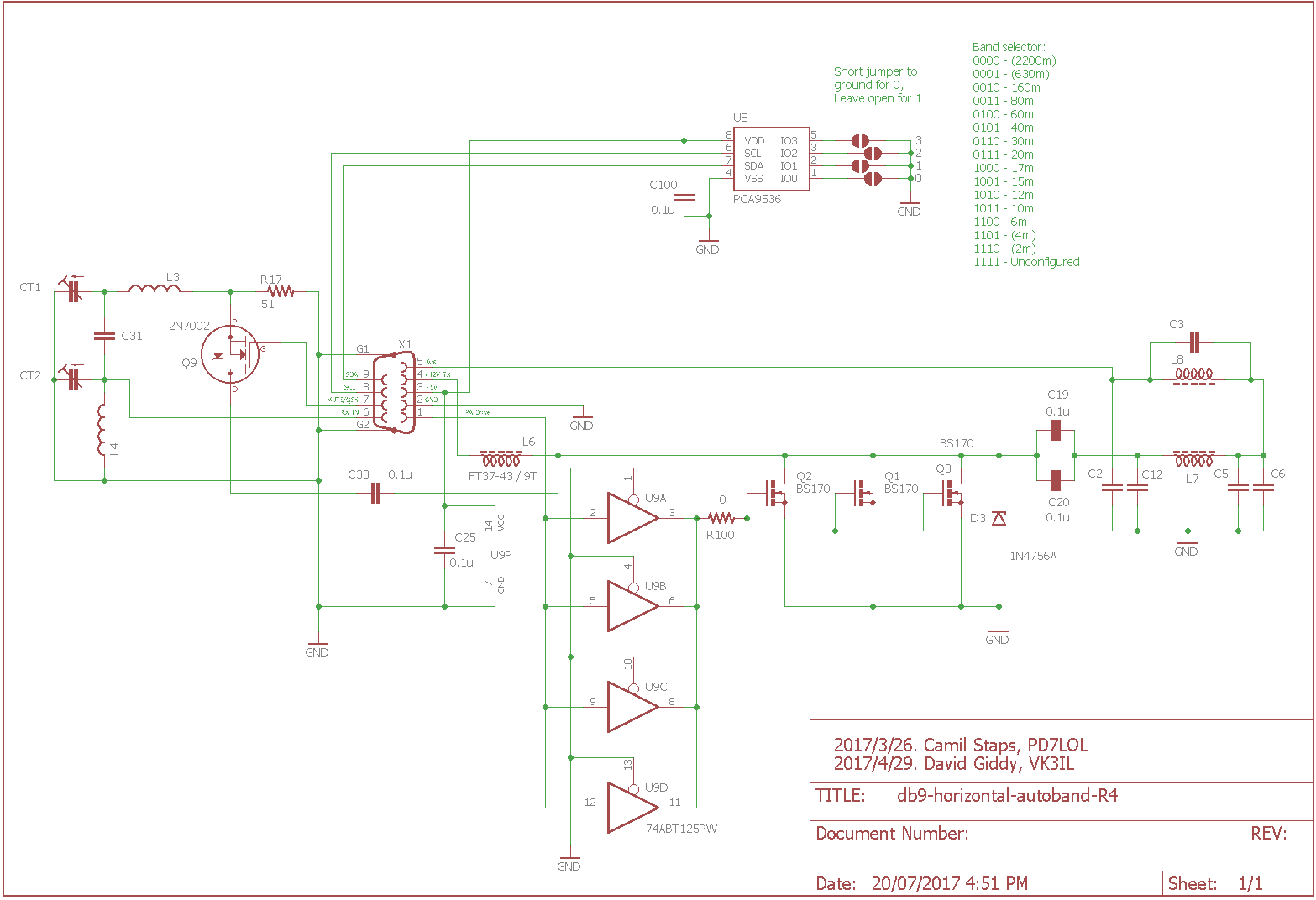
The values of C2, C3, C5, C6,L6, L7, L8, L3, L4, C31, CT1 and CT2 are dependent on the band and the correct values are listed in the detail design section below.
Performance
With tweaking of values, the modules are now all putting out approx 5W at 12V with acceptable spectral emissions. The efficiency is highest at the lower frequencies with the output for each band as follows:
Soda Pop band module performance summary
| Band | Power out [W] | Efficiency (at 12V) |
|---|---|---|
| 160 | 5.8 | 76% |
| 80 | 5.4 | 74% |
| 60 | 5.5 | 74% |
| 40 | 5.6 | 72% |
| 30 | 6.3 | 73% |
| 20 | 6.0 | 70% |
| 17 | 6.9 | 69% |
| 15 | 6.9 | 65% |
| 12 | 4.2 | 46% |
| 10 | 5.0 | 54% |
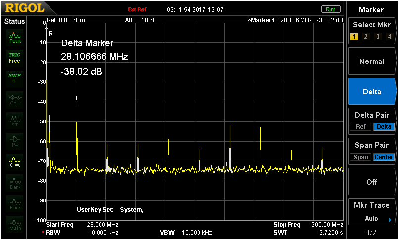
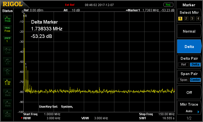
There was some challenge getting the harmonic level down adequately on the 12m and 10m bands due I think to the parasitics in the load networks becoming significant at the harmonics of those bands. The load networks themselves did not provide sufficient harmonic attenuation and so I added an additional 5 pole low pass filter between the module output and the antenna socket. The cut off frequency was set to a little above 50Mhz so that it focused on attenuating the harmonics of 12m and 10m primarily and hopefully would work with a future 6m board addition.
Here is the 10m spectrum without the extra LPF:
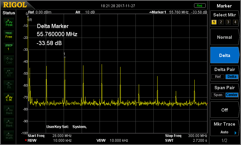
Here is the 10m spectrum with the final LPF:
This has also reduced the higher order harmonics on the lower bands. As an example, the wide spectral response on 160m before the final filter was added was: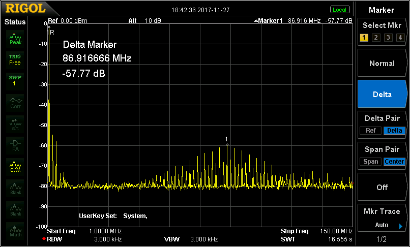
After the final LPF was added it became:
Detailed performance measurements and spectral plots are available here.
Receive performance
The other area of challenge was the receive performance. Again, getting the performance consistent across such a wide frequency range was hard. I found initially that the sensitivity on the higher bands dropped off markedly and traced this primarily to the LO injection level. C43/R29 which acts as a low pass filter. On the higher bands, the signal level at the gate of the mixer dropped below 1V p-p which is not enough to provide good sensitivity. I replaced C43 with a 33pF capacitor, which provided 2.5V p-p on 10m band. The sensitivity still drops off on the higher bands, but is now adequate.
The final measured sensitivities were:
| Frequency [MHz] | MDS (3dB above noise) [dBm] |
|---|---|
| 1.812 | -116 |
| 3.560 | -116 |
| 5.3515 | Better than -120 |
| 7.030 | -116 |
| 10.116 | -116 |
| 14.060 | Better than -120 |
| 18.086 | -110 |
| 21.060 | -106 |
| 24.906 | -106 |
| 28.060 | -96 |
Note that I cannot reliably measure sensitivities better than -120dBm with the equipment I have.
Housing
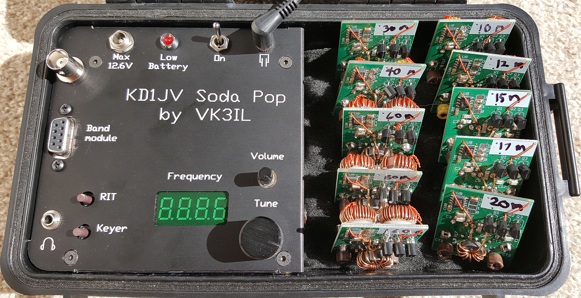
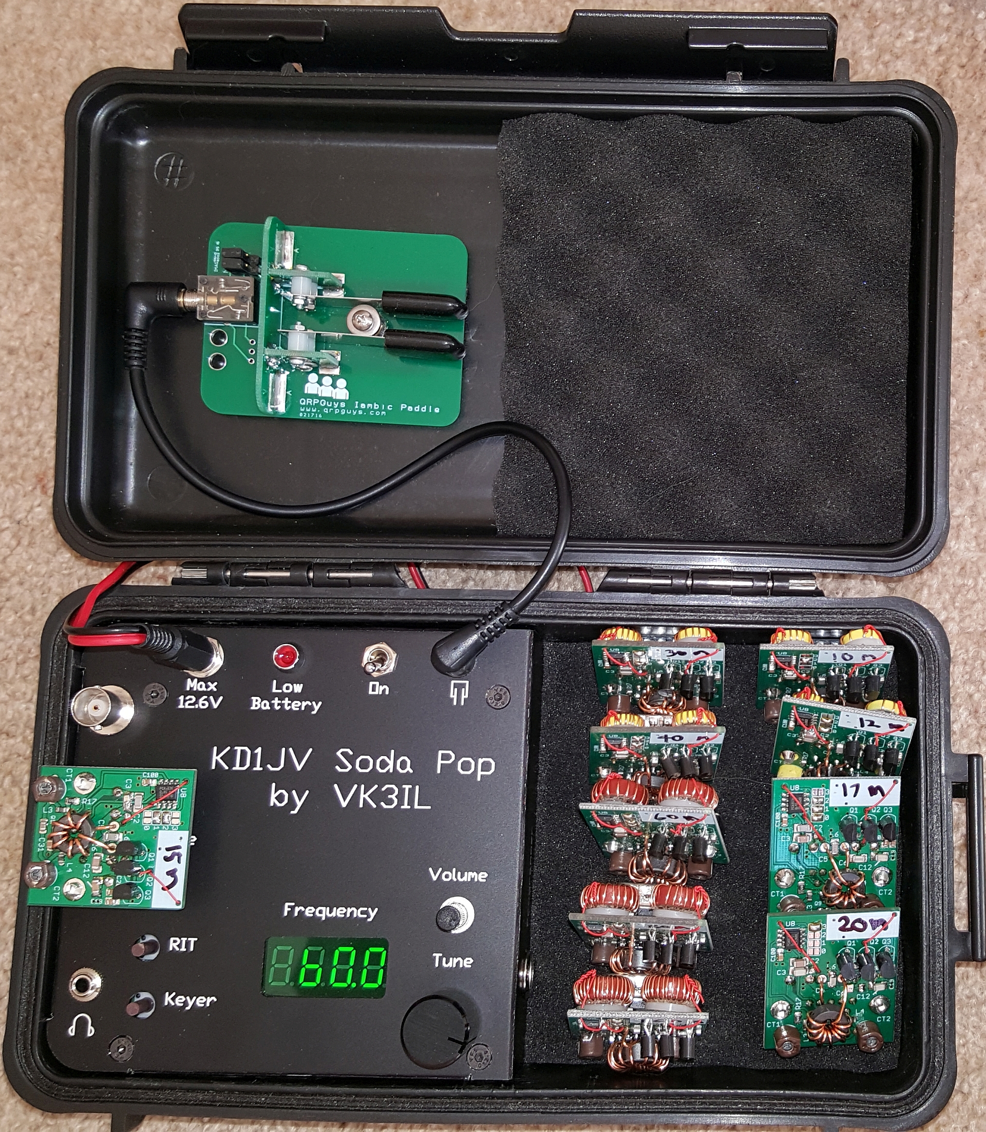
I decided to go for an all-in-one case solution for the Soda Pop. I wanted a case that would need no further protection and would be able to house batteries, band modules, paddle and ear buds leaving only the antenna to be carried separately.
I selected a small Pelican-type case called a “Bob” case – available here. There are likely similar cases available in other countries.
With metalwork not being my strong suit, I designed a front panel to fit the case and had it professionally CNC machined and engraved from black anodised 1.6mm aluminium. This was not cheap, but gave a very nice finish.
I used a 3S 1000mAh LiPo battery together with a BMS board from eBay. I also added a low voltage warning light to give me some warning before the BMS shut off the battery.
Here’s a photo of the final rig together with a QRPGuys CW paddle velcroed to the lid of the case.
Design details
For anyone wanting to duplicate the band modules, here are a few resources and hints.
I have not included the details of the final LPF as I think in practice it is unnecessary. The worst case harmonic is the 3rd harmonic on 10m which peaks at -33.6dBc. Thus at 5W output, the absolute power in this harmonic is 3.4dBm or 2.2mW. This is far below the 74mW that is allowed on a 1500W amplifier harmonic (-43dBc) and unlikely to cause problems for anyone in practice.
Changes required to the main board:
- Remove the following components: CT1, CT2, L3, L4, C31, Q9, R17, C33, Q1, Q2, Q3, D3, C19, C20, C2, C3, C5, C6, C12, L6, L7, L8.
- Do not remove C25 from the main board despite it appearing on the band module board – that’s a component numbering anomoly – both are needed
- Change R50 to 27 ohms (0805 size)
- Change C43 to 33pF (0805 size)
- Attach the DB9 connector as follows:
- Pin 1 – Connect to the gate pad on one of the removed BS170s
- Pin 2 – Connect to a convenient ground pad
- Pin 3 – Connect to a convenient +5V pad
- Pin 4 – Connect to the C25 side of the removed L6
- Pin 5 – Connect direct to the antenna output (use miniature coax if it runs any distance)
- Pin 6 – Connect to the non-grounded pad of the removed CT2 (I used miniature coax for this connection to minimise noise pick up)
- Pin 7 – Connect to the gate pad of the removed Q9 (junction with C28)
- Pin 8 – Connect to the microprocessor pin 28 (use twisted pair with pin 9 wire)
- Pin 9 – Connect to the microprocessor pin 27 (use twisted pair with pin 8 wire or ribbon cable)
PCB gerber files are here. These files are panelised into a 74 x 99mm board containing 6 copies of the board. This is to fit within the prototype limit of 100x100mm that many board houses use. I use allpcb.com for board production as they are very competitive on price for small prototype quantities and good quality.
Here’s a spreadsheet with the values of the band specific components together with a complete BOM.
Here’s a link to a Google drive folder containing photos of the front and back of each module which may help with winding the toroids (particularly initial turn spacing on L7 and L8) and clarification of component installation.
Build notes:
- The parts bags from Digikey have the part number and band on each to help cross check you are putting the correct parts on each module, but cross check against the spreadsheet too
- Don’t forget to use ESD precautions for the semiconductors
- Label the modules by band before you start so that you don’t get confused which one you are working on – you can’t tell which capacitors you’ve installed once they are on the board!
- Assembling the modules in the following order is easiest:
- SMT components on the bottom
- SMT components on the top
- Solder jumpers
- Transistors
- Trimmer caps
- L7, L8 toroids
- DB9 Connector
- L6 toroid
- Zener diode
- Be careful with soldering U9 – the pin pitch is fine and you will get solder bridges. Cleaning up with thin solder wick works well. Inspect carefully with a magnifying glass
- Watch the orientation of U8, pin 1 is identified by a beveled edge on the package which is hard to see. Cross check the orientation against one of my photos to verify
- R100 turned out to be unnecessary, so just bridge the pads
- Wind the toroids using the specified wire sizes and space the windings similar to the photos of my modules and the tuning should be close
- L6 wire is a tight fit to the PCB holes, so don’t pre-tin the ends of this one, just scrape off the enamel and solder directly
- Follow Steve’s alignment procedure for the receive BPF tuning for each module
- Check the output power and adjust by changing the inductance of L7 through adjusting the coil spacing – spreading the turns out will increase the power and bunching them together will decrease it
- I suggest using nylon washers as spacers under the toroids once adjusted – use some hot melt glue to hold them in place to the toroid. For L7, L8, tie the assembly to the board using maybe fishing braid or similar through the 3 holes. L6 can’t be tied, but with 0.8mm wire, it is already quite rigid
The 4 bit I2C PCA9536 to provide a static board id is nice, and replaces explicit band switching. I’ve used PCA8574 I2C 8bit IO expander to switch bands and found it a breeze to set up and use.
Also note you chose a 74ABT125 tristate buffer, I’ve used 74HC04 inverters, not surface mount of course, so not suitable for your project, but I wonder if your part would work at higher frequencies, a consideration when you start to get up there at HF.
Hi Paul,
Yes, I chose the 74ABT125 as a gate driver due to its speed and output current capabilities. To work on 10m, gate drive is the most significant challenge. The 74ABT125 has a propagation delay of only 3-5 ns compared to the 74HC04 which is between 9 and 25 ns. The 74ABT125 can also source and sink more than 32mA per channel (up to 128mA across all 4 outputs) compared to a total of 50mA for the 74HC04 chip. At 30 MHz, you want sub 10ns gate charge time which is possible with this driver. However, I don’t think this is going to work very well at 6m, it’s really too high a frequency for the BS170s.